News
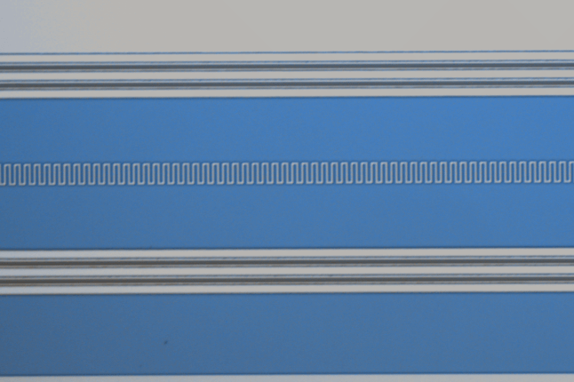
SEAS researchers developed the first in-sensor processor that could be integrated into commercial silicon imaging sensor chips. The array (illustrated here) simplifies image processing for autonomous vehicles and other applications. (Credit: Donhee Ham Research Group/Harvard SEAS)
As any driver knows, accidents can happen in the blink of an eye — so when it comes to the camera system in autonomous vehicles, processing time is critical. The time that it takes for the system to snap an image and deliver the data to the microprocessor for image processing could mean the difference between avoiding an obstacle or getting into a major accident.
In-sensor image processing, in which important features are extracted from raw data by the image sensor itself instead of the separate microprocessor, can speed up the visual processing. To date, demonstrations of in-sensor processing have been limited to emerging research materials which are, at least for now, difficult to incorporate into commercial systems.
Now, researchers from the Harvard John A. Paulson School of Engineering and Applied Sciences (SEAS) have developed the first in-sensor processor that could be integrated into commercial silicon imaging sensor chips ––known as complementary metal-oxide-semiconductor (CMOS) image sensors –– that are used in nearly all commercial devices that need capture visual information, including smartphones.
The research is published in Nature Electronics.
“Our work can harnesses the mainstream semiconductor electronics industry to rapidly bring in-sensor computing to a wide variety of real-world applications,” said Donhee Ham, the Gordon McKay Professor of Electrical Engineering and Applied Physics at SEAS and senior author of the paper.
Ham and his team developed a silicon photodiode array. Commercially-available image sensing chips also have a silicon photodiode array to capture images, but the team’s photodiodes are electrostatically doped, meaning that sensitivity of individual photodiodes, or pixels, to incoming light can be tuned by voltages. An array that connects multiple voltage-tunable photodiodes together can perform an analog version of multiplication and addition operations central to many image processing pipelines, extracting the relevant visual information as soon as the image is captured.
“These dynamic photodiodes can concurrently filter images as they are captured, allowing for the first stage of vision processing to be moved from the microprocessor to the sensor itself,” said Houk Jang, a postdoctoral fellow at SEAS and first author of the paper.
The silicon photodiode array can be programmed into different image filters to remove unnecessary details or noise for various applications. An imaging system in an autonomous vehicle, for example, may call for a high-pass filter to track lane markings, while other applications may call for a filter that blurs for noise reduction.
“Looking ahead, we foresee the use of this silicon-based in-sensor processor not only in machine vision applications, but also in bio-inspired applications, wherein early information processing allows for the co-location of sensor and compute units, like in the brain,” said Henry Hinton, a graduate student at SEAS and co-first author of the paper.
Next, the team aims to increase the density of photodiodes and integrate them with silicon integrated circuits.
“By replacing the standard non-programmable pixels in commercial silicon image sensors with the programmable ones developed here, imaging devices can intelligently trim out unneeded data, thus could be made more efficient in both energy and bandwidth to address the demands of the next generation of sensory applications,” said Jang.
The research was co-authored by Woo-Bin Jung, Min-Hyun Lee, Changhyun Kim, Min Park, Seoung-Ki Lee and Seongjun Park. It was supported by the Samsung Advanced Institute of Technology under Contract A30216 and by the National Science Foundation Science and Technology Center for Integrated Quantum Materials under Contract DMR-1231319.
Topics: Applied Physics, Technology
Cutting-edge science delivered direct to your inbox.
Join the Harvard SEAS mailing list.
Scientist Profiles
Donhee Ham
John A. and Elizabeth S. Armstrong Professor of Engineering and Applied Sciences
Press Contact
Leah Burrows | 617-496-1351 | lburrows@seas.harvard.edu


