News
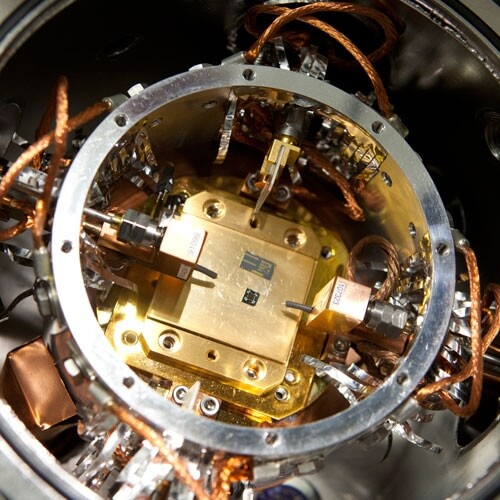
The chamber of the probe station where Donhee Ham's research group tests the new metamaterials. (Photo by Eliza Grinnell, SEAS Communications.)
Cambridge, Mass. - August 1, 2012 - In a vacuum, light travels so fast that it would circle the Earth more than seven times within the blink of an eye. When light propagates through matter, however, it slows by a factor typically less than 5. This factor, called the refractive index, is positive in naturally occurring materials, and it causes light to bend in a particular direction when it shines on, for example, water or glass.
Over the past two decades, scientists have managed to create artificial materials whose refractive indices are negative; these negative-index metamaterials defy normal experience by bending light in the "wrong" direction. Due to their unusual ability to manipulate electromagnetic waves and their potential to be harnessed for technology (that might, for example, cloak objects from view), negative-index metamaterials have been celebrated by scientists and engineers alike.
Researchers at the Harvard School of Engineering and Applied Sciences (SEAS), collaborating with the Weizmann Institute of Science in Israel, have now demonstrated a drastically new way of achieving negative refraction in a metamaterial.
The advance, reported in the August 2 issue of Nature, results in an "extraordinarily strong" negative refractive index as large as -700, more than a hundred times larger than most previously reported.
"This work may bring the science and technology of negative refraction into an astoundingly miniaturized scale, confining the negatively refracting light into an area that is 10,000 times smaller than many previous negative-index metamaterials," says principal investigator Donhee Ham, Gordon McKay Professor of Electrical Engineering and Applied Physics at SEAS.
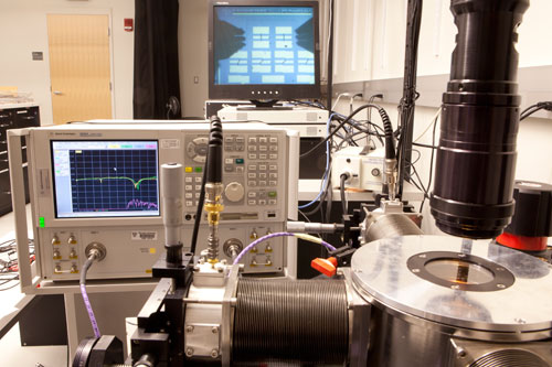
The experimental setup in Donhee Ham's lab shown here is used to test the new metamaterials, which are fabricated on tiny chips. The metamaterials themselves are inside the probing chamber at the bottom right. Imaged through the black microscope, they appear on the screen at the top of this image. (Photo by Eliza Grinnell, SEAS Communications.)
The underlying physics of previous work in this field has often involved an entity called magnetic inductance. Ham's research group instead explored kinetic inductance, which is the manifestation of the acceleration of electrons subjected to electric fields, according to Newton's second law of motion.
At its heart, the researchers' change in strategy from using magneticinductance to kinetic inductance stems from a simple shift in ideas.
"Magnetic inductance represents the tendency of the electromagnetic world to resist change according to Faraday's law," explains Ham. "Kinetic inductance, on the other hand, represents the reluctance to change in the mechanical world, according to Newton's law."
"When electrons are confined perfectly into two dimensions, kinetic inductance becomes much larger than magnetic inductance, and it is this very large two-dimensional kinetic inductance that is responsible for the very strong negative refraction we achieve," explains lead author Hosang Yoon, a graduate student at SEAS. "The dimensionality profoundly affects the condensed-matter electron behaviors, and one of those is the kinetic inductance."
To obtain the large kinetic inductance, Ham and Yoon's work employs a two-dimensional electron gas (2DEG), which forms at the interface of two semiconductors, gallium arsenide and aluminum gallium arsenide. The very "clean" 2DEG sample used in this work was fabricated by coauthor Vladimir Umansky, of the Weizmann Institute.
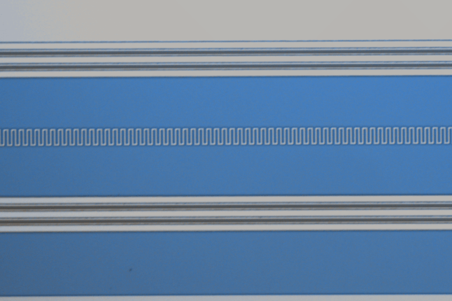
Ham's team effectively sliced a sheet of 2DEG into an array of strips and used gigahertz-frequency electromagnetic waves (microwaves) to accelerate electrons in the leftmost few strips. The resulting movements of electrons in these strips were "felt" by the neighboring strips to the right, where electrons are consequently accelerated.
In this way, the proof-of-concept device propagates an effective wave to the right, in a direction perpendicular to the strips, each of which acts as a kinetic inductor due to the electrons' acceleration therein. This effective wave proved to exhibit what the researchers call a "staggering" degree of negative refraction.
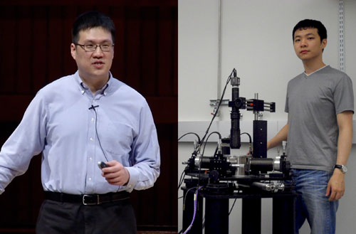
Left: Donhee Ham, Gordon McKay Professor of Electrical Engineering and Applied Physics at SEAS, shown lecturing at the Harvard Thinks Big event. (Photo by Ben Sharbaugh, Harvard News Office.) Right: Ph.D. student Hosang Yoon, a member of Ham's lab and lead author of the paper. Yoon is a graduate of Seoul National University in Korea, where he ranked #1 with a GPA of 4.28 out of 4.30—a feat Ham, who attended the same college, calls "legendary." (Photo courtesy of Hosang Yoon.)
The primary advantages of the new technology are its ability to localize electromagnetic waves into ultra-subwavelength scales and its dramatically reduced size. This concept demonstrated with microwaves, if extended to other regions of the electromagnetic spectrum, may prove important for operating terahertz and photonic circuits far below their usual diffraction limit, and at near field. It may also one day lead to extremely powerful microscopes and optical tweezers, which are used to trap and study minuscule particles like viruses and individual molecules.
For now, the device operates at temperatures below 20 degrees Kelvin. The researchers note, however, that a similar result can be achieved at room temperature using terahertz waves, which Ham's team is already investigating, with the carbon structure graphene as an alternative two-dimensional conductor.
"While electrons in graphene behave like massless particles, they still possess kinetic energy and can exhibit very large kinetic inductance in a non-Newtonian way," says Ham.
Kitty Y. M. Yeung, a graduate student in applied physics at SEAS, also contributed to the work as coauthor.
This research was supported by the Air Force Office of Scientific Research.
Topics: Optics / Photonics, Electrical Engineering, Applied Physics
Cutting-edge science delivered direct to your inbox.
Join the Harvard SEAS mailing list.
Scientist Profiles
Donhee Ham
John A. and Elizabeth S. Armstrong Professor of Engineering and Applied Sciences
Press Contact
Caroline Perry
